
EUV Lithography Proof Is in the Printing
An old adage says, "If you can't measure it, you can't make it." So it's no accident that metrology beamlines built and operated at the ALS under the auspices of Berkeley Lab's Center for X-Ray Optics (CXRO) have been instrumental in a 5-year, $250-million industry–national laboratory effort to bring extreme ultraviolet (EUV) lithography to the commercial stage. EUV lithography is the future chip-printing technology that the Semiconductor Industry Association began backing in 2001 as the likely successor, around the year 2007, to the reigning family of refractive optical lithography techniques. The EUV promise is that with wavelengths 50 times smaller than those of visible light, it will be able to draw circuit patterns just tens of nanometers wide. In comparison, the current industry state-of-the-art chips have patterns with 130-nm lines.
|
Thanks in part to
the CXRO program, interferometry is now routinely used for the
characterization and alignment of optics for EUV lithography,
but the ultimate performance metric remains the quality of the
printed patterns. Moreover, the comparison of a lithographic image
with that predicted from interferometry-derived wavefront maps
is also useful for verifying and improving the predictive power
of wavefront metrology. To address these issues, CXRO added small-field
printing capabilities to the EUV phase-shifting/point diffraction
interferometer (PS/PDI) on ALS Beamline 12.0.1. The first printing
results reveal the extraordinarily high quality of the lithography
optic and in doing so demonstrate the success of CXRO's EUV metrology
beamlines in helping to achieve very tight specifications for
figure, finish, and multilayer coatings of the aspherical mirrors
comprising the lithography optics. 
|
How to Obey Moore's Law
|
||
In the printing configuration, the test station is referred to as the static exposure station (SES). Static means that the scanning and stepping systems required to print complete circuit patterns on all the chips on a silicon wafer are not implemented. Instead, only small ("microfield") test patterns are imaged. Key features of the SES are the ability to control the coherence of the illuminating EUV light (partially coherent is optimum for printing) and the illumination pattern (disk-shaped, annular, dipolar pairs of disks, channel-shaped, etc.). The combined PS/PDI–SES system remains extremely flexible in that switching between the interferometry and printing modes can be accomplished in approximately two weeks. Two 4x reducing optical systems have been developed as part of the EUV lithography program in which Intel, Motorola, Advanced Micro Devices, IBM, Micron Technology, and Infineon Technologies (the EUV Limited Liability Corporation) partnered with the "Virtual National Laboratory," consisting of groups from Lawrence Livermore National Laboratory, Sandia National Laboratories, and Berkeley Lab. The second, much higher quality, Set-2 optic is destined for integration into the prototype printing machine (the Engineering Test Stand or ETS) for full-field scanned imaging, but the CXRO team has already obtained valuable information by using the SES to lithographically characterize the static imaging performance of the Set-2 optic. 
Designed to image features of 100 nm and below in patterns with a dense 1:1 ratio of line widths and line spacing, the ETS Set-2 optic easily lived up to its specs, achieving line widths as narrow as 70 nm in elbow patterns. By adjusting the illumination pattern and the exposure dose, the team printed less densely spaced lines with widths down to 39 nm. These results indicate that with the new optic set expected to arrive at the ALS for testing in November 2002, it should be possible to print features in the 16-nm to 18-nm range and thus meet the production requirements set for chips with 1 billion transistors and up in the years 2007 to 2010. 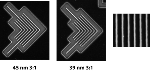
Research
conducted by P.P. Naulleau, K.A. Goldberg, E.H. Anderson, D. Attwood,
P. Batson, P. Denham, E. Gullikson, B. Harteneck, B. Hoef, K. Jackson,
D. Olynick, S. Rekawa, and F. Salmassi (Berkeley Lab); J. Bokor (University
of California, Berkeley, and Berkeley Lab); K. Blaedel, H. Chapman,
L. Hale, R. Soufli, E. Spiller, D. Sweeney, J. Taylor, and C. Walton
(Lawrence Livermore National Laboratory); G. Cardinale, A. Ray-Chaudhuri,
A. Fisher, G. Kubiak, D. O'Connell, R. Stulen, and D. Tichenor (Sandia
National Laboratories); and C.W. Gwyn, P.-Y. Yan, and G. Zhang (Intel
Corporation). |
|||
More ALS Science